Description
The 818 Series are digitally programmable low-pass and high-pass active filters that are tunable over a 256:1 frequency range. 818 filters are available with any one of five standard factory-set tuning ranges or 8-bit custom ranges from 1 kHz. to 1.28 MHz. These units contain 8 CMOS logic inputs.
The 818 Series models are convenient, low profile, easy to use fully finished filters which require no external components or adjustments. They feature low harmonic distortion, and near theoretical amplitude characteristics. 818 filters operate from non-critical ±12 to ±18 Vdc power supplies, have a 5 kΩ (min.) input impedance, a 10 Ω (max.) output impedance and low-pass models offer dc voltage offset adjustment.
Features/Benefits:
- Low harmonic distortion and wide signal-to-noise ratio to 12 bit resolution
- Digitally programmable corner frequency allows selecting cut-off frequencies specific to each application
- Plug-in ready-to-use, reducing engineering design and manufacturing cycle time
- Factory-set tuning range, no external clocks or adjustments needed
- Broad range of transfer characteristics and corner frequencies to meet a wide range of applications
|
|
Applications
- Anti-alias and band-pass filtering
- Data acquisition systems
- Satellite and telecommunications
- Acoustic and vibration analysis and control
- Aerospace, navigation and sonar
- Medical research and electronic equipment
- Engine test and simulation
- Noise elimination
- Video systems
- Signal reconstruction
Available Low-Pass Models:
- 818L8B
- 8-pole Butterworth
- 818L8L
- 8-pole Bessel
- 818L8E
- 8-pole, 6-zero elliptic, 1.77
- 818L8D80
- 8-pole, 6-zero constant delay
Available High-Pass Models:
- 818H8B
- 8-pole Butterworth
- 818H8E
- 8-pole, 6-zero elliptic, 1.77
|
8-Bit Programmable Filters
|
|
818 Series
Digital Tuning &
Control Characteristics
|
|
| Digital Tuning Characteristics
The digital tuning interface circuits are two 4042 quad CMOS latches which accept the following CMOS-compatible inputs: eight tuning bits (D0 - D7 )., a latch strobe bit (C), and a transition
Filter tuning follows the tuning equation given below:
fc = ( fmax/256 ) [ 1 + D7 x 27 + D6 x 26 + D5 x 25 + D4 x 24 + D3 x 23 + D2 x 22 + D1 x 21 + D0 x 20]
where D1 - D7 = "0" or "1", and
fmax = Maximum tuning frequency;
fc = corner frequency;
Minimum tunable frequency = fmax/256 (D0 thru D7 = 0);
Minimum frequency step (Resolution) = fmax/256
|
MSB
|
---
|
---
|
---
|
---
|
---
|
---
|
LSB
|
Bit
Weight
|
27
D7
|
26
D6
|
25
D5
|
24
D4
|
23
D3
|
22
D2
|
21
D1
|
20
D0
|
fc
Corner
Frequency
|
|
0
|
0
|
0
|
0
|
0
|
0
|
0
|
0
|
fmax/256
|
|
0
|
0
|
0
|
0
|
0
|
0
|
0
|
1
|
fmax/128
|
|
0
|
0
|
0
|
0
|
0
|
0
|
1
|
1
|
fmax/64
|
|
0
|
0
|
0
|
0
|
0
|
1
|
1
|
1
|
fmax/32
|
|
0
|
0
|
0
|
0
|
1
|
1
|
1
|
1
|
fmax/16
|
|
0
|
0
|
0
|
1
|
1
|
1
|
1
|
1
|
fmax/8
|
|
0
|
0
|
1
|
1
|
1
|
1
|
1
|
1
|
fmax/4
|
|
0
|
1
|
1
|
1
|
1
|
1
|
1
|
1
|
fmax/2
|
|
1
|
1
|
1
|
1
|
1
|
1
|
1
|
1
|
fmax
|
Data Control Specifications
|
Data Control Lines
|
| Functions |
|
Latch Strobe (C)
Transition Polarity (P) |
|
Data Control Modes
|
| Mode 1 |
|
P = 0; C = 0 frequency follows input codes
P = 0; C = 0Ý frequency latched on rising edge |
| Mode 2 |
|
P = 1; C = 1 frequency follows input codes
P = 1; C = 1ß frequency latched on falling edge |
Notes:
1.Frequency data must be present before occurrence of strobe edge.
2.Frequency data must be present after occurrence of strobe edge.
|
|
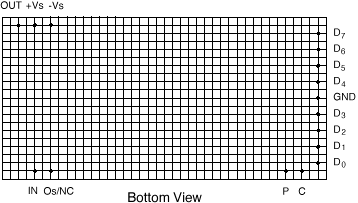
Pin-Out Key
|
IN
|
Analog Input Signal
|
|
D7
|
Tuning Bit 7 (MSB)
|
|
OUT
|
Analog Output Signal
|
|
D6
|
Tuning Bit 6
|
|
GND
|
Power and Signal Return
|
|
D5
|
Tuning Bit 5
|
|
"P"
|
Transition Polarity Bit
|
|
D4
|
Tuning Bit 4
|
|
"C"
|
Tuning Strobe Bit
|
|
D3
|
Tuning Bit 3
|
|
+Vs
|
Supply Voltage, Positive
|
|
D2 |
Tuning Bit 2
|
|
-Vs
|
Supply Voltage, Negative
|
|
D1 |
Tuning Bit 1
|
|
Os
|
Optional Offset Adjustment
|
|
D0 |
Tuning Bit 0 (LSB)
|
|
NC
|
No Connect (Highpass Models)
|
|
|
|
|
Input Data Levels
|
|
(CMOS Logic)
|
| Input Voltage (Vs=15 Vdc ) |
|
|
|
|
| Low Level In |
|
0 Vdc min. |
|
4 Vdc max. |
| High Level In |
|
11 Vdc min. |
|
15 Vdc max. |
| Input Current |
|
|
|
|
| High Level In |
|
-10-5 µA typ. |
|
-1 µA max. |
| Low Level In |
|
+10-5 µA typ. |
|
+1 µA max. |
| Input Capacitance |
|
5 pF typ |
|
7.5 pF max. |
| Latch Response |
|
|
|
|
| Data Set Up Time1 |
|
25 nS |
|
|
| Data Hold Time2 |
|
50 nS |
|
|
| Strobe Pulse Width |
|
80 nS min. |
|
|
|
Input Data Format
|
|
Frequency Select Bits
|
| Positive Logic |
|
Logic "1" = +Vs |
| |
|
Logic "0" = Gnd |
| Bit Weighting |
|
(Binary-Coded) |
| D0 |
|
LSB (least significant bit) |
| D7 |
|
MSB (most significant bit) |
| Frequency Range |
|
256 : 1, Binary Weighted |
|
8-Bit Programmable 8-Pole Low-Pass Filters
| Model |
818L8B |
818L8L |
818L8E |
818L8D80 |
| Product Specifications |
| Transfer Function
Size
Range fc |
8-Pole
Butterworth
2.0” x 4.0” x 0.4”
1 kHz to 1.28 MHz |
8-Pole
Bessel
2.0” x 4.0” x 0.4”
1 kHz to 1.28 MHz |
8-Pole, 6 zero
Elliptic
2.0” x 4.0” x 0.4”
1 kHz to 1.28 MHz |
8-Pole, 6 zero
Constant Delay
2.0” x 4.0” x 0.4”
1 kHz to 1.28 MHz |
Theoretical Transfer
Characteristics |
Click to view
|
Click to view
|
Click to view
|
Click to view
|
Passband Ripple
(theoretical) |
0.0 dB |
0.0 dB |
± 0.035 dB |
0.15 dB |
DC Voltage Gain
(non-inverting) |
0 ± 0.1 dB max.
0 ± 0.05 dB typ. |
0 ± 0.1 dB max.
0 ± 0.05 dB typ. |
0 ± 0.1 dB max.
0 ± 0.05 dB typ. |
0 ± 0.1 dB max.
0 ± 0.05 dB typ. |
Stopband
Attenuation Rate |
48 dB/octave |
48 dB/octave |
80 dB min. |
80 dB min. |
Cutoff Frequency
Stability
Amplitude
Phase |
fc ± 3% max.
± 0.01% /°c
-3 dB
-360° |
fc ± 3% max.
± 0.01% /°c
-3 dB
-182° |
fr ± 3% max.
± 0.01% /°c
-3 dB
-323.5° |
fc ± 3% max.
± 0.01% /°c
-3 dB
-306° |
Filter Attenuation
(theoretical) |
0.12 dB 0.80 fc
3.01 dB 1.00 fc
60.0 dB 2.37 fc
80.0 dB 3.16 fc |
1.91 dB 0.80 fc
3.01 dB 1.00 fc
60.0 dB 4.52 fc
80.0 dB 6.07 fc |
0.035 dB 1.00 fr
3.01 dB 1.13 fr
60.0 dB 1.67 fr
80.0 dB 1.77 fr |
3.01 dB 1.00 fc
60.0 dB 3.08 fc
80.0 dB 3.57 fc |
| Phase Match1 |
- (See below)
|
- (See below)
|
- (See below)
|
- (See below)
|
Amplitude Accuracy
(theoretical) |
- 0 - 0.6 fc
- ± 0.5 dB max.
± 0.25 dB typ.
- 0.6 fc - 1.0 fc
- ± 1.0 dB max.
± 0.6 dB typ.
|
- 0 - fc
- ± 0.8 dB max.
± 0.4 dB typ.
|
- 0 - 0.8 fr
- ± 0.5 dB max.
± 0.25 dB typ.
- 0.8 fr - 1.0 fr
- ± 1.0 dB max.
± 0.5 dB typ.
|
- 0 - 0.8 fc
- ± 0.5 dB max.
± 0.25 dB typ.
- 0.8 fr - 1.0 fc
- ± 1.0 dB max.
± 0.5 dB typ.
|
Total Harmonic
Distortion @ 1 kHz |
< - 88 dB typ. |
< - 88 dB typ. |
< - 88 dB typ. |
< - 88 dB typ. |
Wide Band Noise
(5 Hz - 2 MHz) |
300 µVrms typ. |
300 µVrms typ. |
350 µVrms typ. |
350 µVrms typ. |
Narrow Band Noise
(5 Hz - 100 kHz) |
75 µVrms typ. |
75 µVrms typ. |
75 µVrms typ. |
75 µVrms typ. |
Filter Mounting
Assembly |
FMA-04A |
FMA-04A |
FMA-04A |
FMA-04A |
1. Unit to unit match for the same transfer function, set to the same frequency and operating configuration, and from the same manufacturing lot. |
8-Bit Programmable 8-Pole High-Pass Filters
| Model |
818H8B |
818H8E |
| Product Specifications |
| Transfer Function
Size
Range fc |
8-Pole
Butterworth
2.0” x 4.0” x 0.4”
1.0 Hz to 1.28 MHz |
8-Pole, 6 zero
Elliptic
2.0” x 4.0” x 0.4”
1.0 Hz to 1.28 MHz |
Theoretical Transfer
Characteristics |
Click to view
|
Click to view
|
Passband Ripple
(theoretical) |
0.0 dB |
± 0.035 dB |
Voltage Gain
(non-inverting) |
0 ± 0.5 dB to 1.28MHz |
0 ± 0.5 dB to 1.28MHz |
| Power Bandwidth |
(-6 dB) 5 MHz |
(-6 dB) 5 MHz |
Stopband
Attenuation Rate |
48 dB/octave |
80 dB |
Cutoff Frequency
Stability
Amplitude
Phase |
fc ± 3% max.
± 0.01% /°c
-3 dB
-360° |
fr ± 3% max.
± 0.01% /°c
-0.035 dB
-323.5° |
Filter Attenuation
(theoretical) |
80 dB 0.31 fc
60.0 dB 0.42 fc
3.01 dB 1.00 fc
0.00 dB 2.00 fc |
80 dB 0.56 fr
60.0 dB 0.60 fr
3.01 dB 0.88 fr
0.03 dB 1.00 fr
0.00 dB 2.00 fr |
Amplitude Accuracy
(theoretical) |
- 1.0 - 1.25 fc
- ± 0.5 dB max.
± 0.3 dB typ.
- 1.25 fc - 1.28MHz
- ± 1.0 dB max.
± 0.5 dB typ.
|
- 1.0 - 1.25 fr
- ± 0.5 dB max.
± 0.3 dB typ.
- 1.25 fr - 1.28MHz
- ± 1.0 dB max.
± 0.5 dB typ.
|
Total Harmonic
Distortion @ 1 kHz |
< - 100 dB typ. |
< - 88 dB typ. |
| Wide Band Noise |
400 µVrms typ. |
450 µVrms typ. |
| Narrow Band Noise |
100 µVrms typ. |
100 µVrms typ. |
Filter Mounting
Assembly |
FMA-04A |
FMA-04A |
1. Unit to unit match for the same transfer function, set to the same frequency and operating configuration, and from the same manufacturing lot. |
1 kHz to 1.28 MHz
|
|
818 Series
Phase and Phases
Match Considerations
|
|
| Phase Deviation from Theoretical:
The phase response of the amplifiers and the capacitance of the frequency control switches of the 818 series contribute to the overall phase response and cause it to deviate from theoretical. For the higher frequency models ( -4 and -5 ), where the cutoff frequencies can be programmed up to 1.28MHz, the deviation from theoretical can be substantial.
Figure 1 is a normalized plot of the phase deviation from theoretical for an 818L8E-5 for programmed cutoff frequencies from 5kHz ( fc min ) to 1.28MHz (fc max ). For fc of 5kHz, the deviation from the 323° theoretical phase shift is 2° but for fc of 1.28MHz the deviation is 78°. This set of curves can be used to estimate the deviation from theoretical phase for other models in the 818 series.
Figure 1 represents a "maximum deviation from theoretical phase" situation. Other models (i.e. -1 to -4) will exhibit a similar set of phase deviation curves with the phase scale being reduced by the ratio of the f max of the model to the f max of the -5. For example, an L8E-1, whose programming frequency range is from 1kHz to 256kHz (1/5 of the range of the -5 model) will have a similar set of phase deviation curves but the maximum phase deviation, at the highest frequency setting (fc max), will be approximately 1/5 that of the -5 model (78/5 = 15.6°). The other programmed settings of the -1 will also produce proportionally reduced phase deviations.
Unit to Unit Phase Match2
The actual phase shift through a filter at a frequency " f " is determined by its programmed frequency " fc ", the theoretical phase response of the transfer function (B, L, E, or D80) and the phase deviation from theoretical which in turn depends upon component tolerances, the model # (i.e. -1 through -5) and frequency to which it is programmed. It is therefore not possible to have a meaningful unit to unit phase match that is specified by a single number.
For a group of the same model type and number, programmed to the same frequency, the unit to unit phase match can be approximated as a percentage of the theoretical phase shift with a correction term added to accommodate amplifier induced phase deviations. |
|
EXAMPLE: Phase Match Calculation
  (f)max = 0.02° x (f)max = 0.02° x (f) (f) |
+ 4.0° x f/fc x fmax/1.28MHz |
| |
 |
| |
|
|
| |
|
|
| |
|
4.0° - L8L
3.0° - L8B & L8D80
2.0° - L8L |
(f)typ =0.5 x (f)max
where:
Eg. - for an 818L8E-3, the phase deviation from theoretical at a frequency of 192kHz, when the cutoff frequency fc is programmed to 384kHz is:
f/fc = 192kHz/384kHz = 0.5, fmax = 768kHz
(f) = 133° (from data table at f/fc = 0.5)
Phase Match:
(f)max = 0.02° x (f) + 4.0° x f/fc x fmax/1.28MHz
818L8E Phase Deviation (in degrees “°”) from Theoretical vs. Normalized Input Frequency
programmed setting of fc
| f/fc |
5kHz |
10kHz |
20kHz |
40kHz |
80kHz |
160kHz |
320kHz |
640kHz |
1.28MHz |
|
0.10
|
0.15
|
0.18
|
0.17
|
0.08
|
-0.12
|
-0.52
|
-1.18
|
-2.57
|
-5.32
|
|
0.20
|
0.30
|
0.32
|
0.30
|
0.17
|
-0.39
|
-1.03
|
-2.41
|
-5.17
|
-10.76
|
|
0.30
|
0.34
|
0.42
|
0.40
|
-0.18
|
-0.57
|
-1.59
|
-3.66
|
-7.89
|
-16.29
|
|
0.40
|
0.20
|
0.40
|
0.50
|
-0.20
|
-0.90
|
-2.30
|
-5.10
|
-10.80
|
-22.10
|
|
0.50
|
0.20
|
0.32
|
0.60
|
-0.40
|
-1.20
|
-3.00
|
-6.70
|
-14.00
|
-28.20
|
|
0.60
|
0.00
|
0.00
|
-0.10
|
-0.80
|
-1.90
|
-4.10
|
-8.70
|
-17.70
|
-35.10
|
|
0.70
|
-0.21
|
-0.30
|
-0.60
|
-1.30
|
-2.70
|
-5.40
|
-11.00
|
-21.80
|
-42.60
|
|
0.80
|
-0.50
|
-0.60
|
-1.30
|
-2.10
|
-3.80
|
-7.20
|
-13.90
|
-26.90
|
-51.30
|
|
0.85
|
-0.80
|
-1.00
|
-1.80
|
-2.80
|
-4.70
|
-8.40
|
-15.80
|
-30.10
|
-56.40
|
|
0.90
|
-1.20
|
-1.60
|
-2.50
|
-3.70
|
-5.80
|
-10.00
|
-18.40
|
-33.80
|
-62.30
|
|
0.95
|
-1.90
|
-2.40
|
-3.50
|
-4.80
|
-7.30
|
-12.00
|
-21.10
|
- 38.30
|
-69.20
|
|
1.00
|
-2.50
|
-3.30
|
-4.60
|
-6.20
|
-8.90
|
-14.10
|
-24.30
|
-43.30
|
-77.50
|
|
Phase Deviation from Theoretical

Specifications
(@ 25°C and Vs ±15 Vdc)
|
Analog Input Characteristics1
- Impedance: 5 kΩ min.
- Voltage Range: ± 10 Vpeak
- Max. Safe Voltage: ± Vs
Analog Output Characteristics
- Impedance(Closed Loop):
1 Ω typ.
10 Ω max.
- Linear Operating Range: ± 10 V
- Maximum Current2: ± 5 mA
- Offset Voltage3:
2 mV typ.
10 mV max.
- Offset Temp. Coeff.: 50 µV / °C
Notes:
- Input and output signal voltage referenced to supply common.
- Output is short circuit protected to common. DO NOT CONNECT TO +/-Vs.
- Adjustable to zero
- Units operate with or without offset pin connected.
|
Power Supply (+/-V)
- Rated Voltage: ± 15 Vdc
- Operating Range: ± 12 to ± 18 Vdc
- Maximum Safe Voltage: ± 18 Vdc
- Quiescent Current:
100 mA typ
120 mA max.
Temperature
- Operating: 0 to + 70°C
- Storage: -25 to+85°C

|
Pin-Out and Package Data

Filter Mounting Assembly-See FMA-04A
Ordering Information

|
Model Number
|
Tuning Range (Hz)
|
Minimum Step (kHz)
|
1
|
1kHz to 256kHz
|
1kHz
|
2
|
2kHz to 512kHz
|
2kHz
|
3
|
3kHz to 768kHz
|
3kHz
|
4
|
4kHz to 1,024kHz
|
4kHz
|
5
|
5kHz to 1,280kHz
|
5kHz
|
Power Sequence & ESD
Programmable Filters Modules
- Scope
The following precautions are necessary when handling and installing Frequency Devices programmable filter modules.
- Digital Circuit Description
The digital input pins connect directly to 4000 series CMOS logic, such as the 4053 analog switch. The power supply (Vss) for the digital logic on the module comes directly from the +15 Volt pin on the module. This sets the threshold voltage at 11.0 V minimum to 15.0 V maximum for a "1" (High) level and 0.0 V minimum to 4.0 V maximum for a "0" (Low) level. Applying a voltage between 4.0 and 11.0 V will produce unpredictable operation. Connecting 5 Volt or 3.3 V logic devices directly to the filter module without using a voltage translator will result in erratic operation of the filter.
- (VERY IMPORTANT) Power-Up and Power-Down Sequence
Do not plug-in or un-plug module while power is applied. It is imperative that power is supplied to the + 15 V pin on the filter module before or at the same instance that any digital pin is pulled High (> 0.0 V). Failure to do this will result in excessive current flowing through the digital input pin and through a protection diode internal to the 4000 logic, which will result in damage to the module. The proper power-up and power-down sequence is:
- Connect filter module ground.
- Connect filter module +15 V.
- Connect filter module -15 V.
- Connect the input signal.
All four of the above steps can also occur simultaneously. Power-down should occur in the reverse order.
- ESD Issues
Like most modern electronic equipment, the modules can be damaged by electrostatic discharge (ESD). The modules are shipped from the factory in sealed, anti-static packaging and should be kept in the sealed package prior to mounting on a circuit board. The following additional rules should also be observed when handling the modules after they are removed from the factory packaging:
- Only a person wearing a properly grounded wrist strap should handle the modules.
- Any work surface that the modules are placed on must be properly ESD grounded.
- Any insulating materials capable of generating static charge (such as paper) should be kept away from the modules.
We hope the information given here will be helpful. The information is based on data and our best knowledge, and we consider the information to be true and accurate. Please read all statements, recommendations or suggestions herein in conjunction with our conditions of sale which apply to all goods supplied by us. We assume no responsibility for the use of these statements, recommendations or suggestions, nor do we intend them as a recommendation for any use which would infringe any patent or copyright.
|